
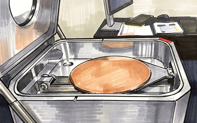

- 01200mm graphene deposition achieved below 300°C on a 314 cm2 wafer.
- 0212 wafer sites across four quadrants confirm graphene via Raman.
- 03Path to collabs/licensing.
Adisyn (ASX: AI1) has achieved a major technical milestone in the development of its graphene semiconductor technology, scaling its low-temperature deposition process to a full 200-millimetre copper semiconductor wafer.
The deposition was completed below 300° Celsius on a surface area of approximately 314 square centimetres—approximately 300 times larger than Adisyn’s previously announced process result.
Following deposition, 12 sampling locations were selected across all four quadrants of the wafer at varying distances from its centre with each location measured five times using Raman spectroscopy to identify and characterise the deposited graphene.
The locations were then examined at the Hebrew University of Jerusalem using transmission electron microscopy to provide complementary nanoscale analysis.
The transition to a full 200mm semiconductor wafer represents a a substantial increase in the area coated in a single deposition run and a significant scale-up of Adisyn’s graphene deposition technology platform.
Exceeded Expectations
Managing director Arye Kohavi said the milestone was ahead of the company’s internal development expectations and demonstrated the rapid progress of its graphene semiconductor program.
“Scaling a new materials technology from laboratory samples to a full 200mm semiconductor wafer presents significant technical challenges,” he said.
“Achieving that step—and identifying graphene at all 12 locations independently tested across the wafer—provides important validation of our technology and development approach.”
Adisysn believes this will provide it with a foundation to further assess uniformity, defectivity, and reproducibility, as well as determine initial first-pass reliability data in various applications and pursue joint development programs with semiconductor manufacturers.
Semiconductor Strengths
Graphene is being investigated globally for semiconductor interconnects and hybrid graphene metal structures due to its electrical conductivity, thermal properties, and potential to improve the performance and reliability of increasingly small interconnected structures.
These challenges are particularly relevant to advanced AI, high-performance computing, and memory devices predominantly manufactured on 300mm wafers and Adisyn’s 200mm result represents an important pathfinder towards achieving that format.
Mr Kohavi believed a successful integration of the company’s process technology platform would create commercial opportunities through potential licencing, joint development, process or materials supply models.
“Complete industrial wafer coverage is a critical goal that we expected to achieve in just a few months, and meeting it today shortens the planned timelines for industry collaborations and integrations,” he added.
Get the wire before the market opens.
The ASX small-cap stories that matter, filed before 9am AEST. Curated by the Small Caps desk.